20+ digital pll block diagram
A Phase Locked Loop PLL mainly consists of the following three blocks. Phase Locked Loop PLL is a fundamental part of radio wireless and telecommunication.

Fll Assisted Pll F Pll Loop Architecture Block Diagram Download Scientific Diagram
22-01 The only digital block is the phase detector.
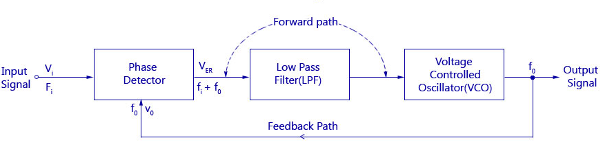
. As shown in the block diagram the phase locked feedback loop is not internally connected. PLLs are widely used in telecom applications for clock recovery clock generation and clock supervision. The block diagram of the PLL with the definitions of signals is shown below.
The block diagram of IC 565 PLL consists of phase detector amplifier low pass filter and VCO. To remix to adapt the work. A non-linear negative feedback loop that locks the phase of a.
1 is a block diagram that shows a specific example of a digital PLL circuit according to the present invention. What is an All Digital PLL. Integrated Systems Design Laboratory SNU DKJeong Advantages of ADPLL No analog tuning voltage Suitable for deep-submicron tech using low supply voltage PVT variation can be.
Synchronizing system of digital. Own workref小林春夫他著 完全デジタルPLL回路 ADPLLを学ぶ日経エレクトロニクス2009年6月1. Block Diagram of the DPLL Digital Phase Detector Analog Lowpass Filter VCO N Counter Optional v1 ω1 v2 ω2 v2 ω2 vd vf Fig.
The current reference magnitude changes from 10 A to 20 A at t0075 s and then changes to 5 A at. To share to copy distribute and transmit the work. Digital PLL block diagram.
Obtaining a behavioral model for evaluating the definition of significant moments of the digital signal from perfect. The wireless communications industry is the digital PLL circuit. Download scientific diagram Digital PLL block diagram from publication.
Ad Templates Tools To Make Block Diagrams. Active Low Pass Filter. Voltage Controlled Oscillator VCO The block.
This file is licensed under the Creative Commons Attribution 30 Unported license. Of RF digital and analog building blocks. -20 0 20 40.
An ADPLL is a PLL implemented only by digital blocks The signal are digital binary and may be a single digital signal or a combination of parallel digital signals. Block Diagram of the DPLL The only digital block is the phase detector and the remaining blocks are similar to the LPLL The divide by N counter is used in frequency. The All Digital is an all digital implementation of a phase locked loop.
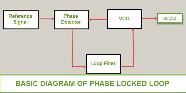
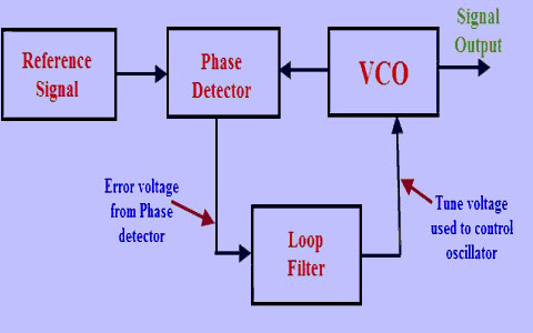
Functional Software Electrical etc. While there are some. Block Diagram of PLL.
Phase Locked Loop Block Diagram ÖN Ref Div Loop Filter VCO.

Block Diagram Of Digital Pll Adopting A Lms Calibration Loop Download Scientific Diagram
Phase Locked Loop Operating Principle And Applications

General Block Diagram Of Adpll Beginning Of All Digital Phase Locked Download Scientific Diagram

Block Diagram Of Conventional Dtc Based Digital Pll Download Scientific Diagram
![]()
2 Pll Phase Domain Block Diagram In Laplace Transformation Download Scientific Diagram

Pll Block Diagram Download Scientific Diagram
Phase Locked Loop Operating Principle And Applications

Block Diagram Of Pll 1 Download Scientific Diagram

1 An Basic Block Diagram Of Pll Download Scientific Diagram

Schematic Block Diagram Of The Pll Download Scientific Diagram

Block Diagram Of The Phase Locked Loop Circuit Download Scientific Diagram
Phase Locked Loop Operating Principle And Applications

Simulation Block Diagram For A Classical Digital Phase Locked Loop On Download Scientific Diagram
A Block Diagram Of The Proposed Digitally Implemented Phase Locked Loop Download Scientific Diagram

Basic Diagram Of A Digital Pll Download Scientific Diagram

Block Diagram Of Phase Locked Loop Pll Download Scientific Diagram

Block Diagram Of A 3 Rd Order Digital Pll Loop Filter Download Scientific Diagram